Adjustment method
Main power +B setting
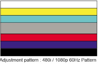
Receive standard color
pattern RF signal, set picture to “ Standard
Mode” . Adjust VR501. to get +B (VD631 -) voltage =110 V
I2C bus control adjustment method:
enter and exit factory mode
For remote controller of factory
Continuous push [test]
key on the remote controller, the TV
mode will change as: Normal è
M è BUS OPEN
You can select “M” ( factory mode ) or
“normal” mode.
For remote controller of
user
Push [menu] key, → display picture manual → push digital key 8500 → display M. Push [standby] key,
exit factory mode and TV will be standby.
MENU 8 Geometrical adjustments.
Receive standard Crosshatch pattern signal for PAL system .
Horizontal line
Shadow
1) Adjust VSLOPE value, to the horizontal line just appear from half bottom shadow.
2) Adjust VSHIFT value, the centre horizontal line correspond to CRT vertical centre.
3) Adjust Vamp value, to get 90% of vertical picture contents would be displayed on CRT.
4) Adjust HSHIFT value, to get the picture horizontal centre correspond to CRT horizontal centre.
5) Receive standard Crosshatch pattern signal for NTSC system, and again
adjust.
MENU 7 AGC-TOP adjustment
Receive
60dBu (1mv)VH colour bar signal, adjust AGC value(voltage from high to low), to picture noise reduce gradually to be just disappeared.
MENU 9 CRT cut-off and
white balance and sub-brightness adjustment.
Receive
gray and white 2 steps signal.
a) CRT cut off adjustment.
1. push [▲P+][▼P-] key to select “SC”, push [►V+][◄V-] key then automatically
vertical scan will be stopped.
2. Adjust SCREEN control on Flyback transformer to get the darkest single
horizontal line (red、green, or blue, sometimes shows more yellow、more purple or more white).
3. Push [V+][V-] key again, vertical scan work repeat.
b) White balance
adjustment.
1. Select RD/BD menu.
2. Adjustment RD/BD to get color temperature as x=281, y=311.
c) sub-brightness adjustment (use stair case signal)
1. Select SB MENU.
2. Adjust SB to get the darkest step being on or off.
MENU 6 Set SHIP MODE
Select
“SHIPMODE”, push [V+][V-]key may be
shipped.
Note:: may increase the screen of FBT current, the darkling single ought no fly
back line, AV state.
I2C bus control
adjustment item default setting (21 inch)


Note1:
TEXT DEF : TXT_def = 0: Pan_Euro + Cyrillic
= 1: Farsi English + French + Turkish
= 2: Arabic + English + French + Turkish
= 3: UKRAINIAN
Attention:
When TXT_def=0, will appear" the TXT LANGUAGE" in the customer Setup
menu, press V+/ V- key," the TXT LANGUAGE" will appear the following
circulation: W- TR-> EAST1-> EAST2-> W- TR
The W- TR diagram text includes the following language:
English German Swedish/Fin/Dan/Hungarian Italian French Spanish/Portuguese
Turkish The EAST1 diagram text includes the following language:
Polish German Estonian Slovenian Czech/Slovak Rumanian
The EAST2 diagram text includes the following language:
Polish German Swedish/Fin/Dan/Hungarian Lettish Russian Slovenian Czech/Slovak
Estonian
Note 2:
Make use of 4 color keys of the remote control, browse 4 pages of the enactment
quickly, namely index function.
The TV/ AV sets the saving key for the index.
While using this function," the TXT LIST" establishes for"
ON" in the customer menu.
Example: if want to use the color key of the red quickly 230 pages of enter the
diagram text
The sequence press" TEXT"," red
key","2","3","0" on the remote
control," TV/ AV"
Note 3:
Switch on the hour appearance constitution
0: connect the AC power, enter to need the machine appearance automatically
1: connect the AC power, automatically switch on appearance
2: connect the AC power, if shut down the appearance as the diagram text appearance,
enter the diagram text appearance automatically.
SCHEMATIC DIAGRAM

The main chips
instruction. TDA93X1
The UOC (“Ultimate One Chip”) TDA93X1 is adopted in this chassis. This IC is
the first available component that contains the complete control and small
signal functionality needed for a TV application in one device.
The UOC TDA93X1 pins function description:(total 64 pins)
Pin1:
Standby control,“ 1” is on,“ 0” is off.
Pin2: SCL.
Pin3: SDA.
Pin4: Tuning PWM output.
Pin5: Auto AV control SW/NTSC SW,
Pin6: Key board input.
Pin7: Volume
Pin8: Mute control,“ 1” is mute,“ 0” is off.
Pin9: Pin12, Pin18, Pin30, Pin35, Pin41, Pin55: GND.
Pin10: BAND1 control output.
Pin11: BAND2
Pin12: GND
Pin13: SECAM PLL, connected with a capacitance.
Pin14: +8V power source
supply.
Pin15: Using a capacitor of 220n in series to GND, This pin decouples the
internal digital supply voltage of the video processor and minimizes the
disturbance to the sensitive analogue parts.
Pin16: PHI-2 control loop, this pin requires a capacitor at 2.2nF (C) in series
to GND.
Pin17: PHI-1 control loop, the loop filter connected to pin 17 is suitable for
various signal conditions strong/weak
and VCR signal. This is achieved by switching of the loop filter time constant y
changing the PHI-1 output current.
Pin18: GND.
Pin19: Band gap decoupling, the band gap circuit provides a very stable and
temperature independent reference voltage. This reference voltage (4.0 V)
ensures optimal performance of the analogue video processor part of the N301
and is used in almost all functional circuit blocks.
Pin20: East-west pillow signal output.
Pin21: Pin22: Vertical drive output.
Pin23: Pin24: IF input。
Pin25:
Reference current, This pin requires a resistor to ground. The optimal
reference current is 100mA which is determined by this resistor. The 100mA
reference current should not be changed because the geometry processor is
optimised for this current. Furthermore the output current of vertical drive
and EW are proportional to this current.
Pin26: Vertical saw tooth, This pin requires a capacitor to ground of 100nF
Pin27: AGC output. This output is used to control (reduce) the tuner gain for
strong RF signals.
Pin28: Audio de-emphasis.
Pin29: Sound decoupling. This pin requires a capacitor connected to ground. The
pin acts as a low pass filter needed for the DC feedback loop.
Pin30: GND.
Pin31: Sound loop filter.
Pin32: AVL filter.
Pin33: Horizontal drive signal output, needs a resistor in series to +8V.
Pin34: Sandcastle output/fly back input,
Pin35: External audio input, this pin should be grounded in this chassis.
Pin36: EHT tracking/ overvoltage protection. If something is wrong, the anode
high voltage rises, the heater voltage will rise too. When the rising voltage
arrive some limit, the VD461 works, the voltage of pin 36 will exceed 3.9V, the
N301will stop working.
Pin37: PLL loop filter.
Pin38: CVBS output. Monitor or RF videos can be selected.
Pin39: +8V supply source.
Pin40: CVBS input
Pin42: Y signal input.
Pin43: C signal input.
Pin44: Main audio output
Pin45: RGB signal input blanking.
Pin46, Pin47, Pin48: RGB signal input.
Pin49: ABL. It means been current limiter input. The R464 is the control
resister.
Pin50: Black current input from the CRT board.
Pin51, Pin52, Pin53: RGB drive signal output to the CRT board.
Pin54: +3.3V.
Pin55: GND.
Pin56: +3.3V.
Pin57, Pin58, Pin59: 12MHz crystal。
Pin60:
Reset, NC in this chassis.
Pin61: +3.3V
Pin62: This pin is connected to the HEF4052, Functions expanding.
Pin63: This pin is connected to the HEF4052, Functions expanding.
Pin64: IR signal input.

Memory AT24C08 is an E2PROM of 8k, pins describe as follows:
Pin1, Pin2, Pin3,Pin4, Pin7: GND. Pin8: +5V supply.
Pin5: SDA. Pin6: SCL.